

Abstract
The strontium iridate family includes both conducting and insulating phases with strong spin–orbit coupling. These materials can serve as interlayers in superconducting heterostructures. An epitaxial SrIrO3 film grown on an NdGaO3 substrate exhibited weakly nonmetallic resistivity and an approximately linear Hall response. A single-band analysis at 5 K yielded a carrier density of 2 × 1021 cm−3, a resistivity of 6 × 10⁻³ Ω cm, and a mobility of 0.6 cm2 V−1 s−1. We fabricated Nb/iridate/YBa2Cu3O7−δ superconducting mesa heterostructures. For heterostructures containing 15-nm SrIrO3 interlayers, IcRN was 0.1–0.3 μV at 4.2 K. The corresponding magnetic diffraction pattern had minima close to zero and a Fraunhofer-like central lobe. For 5-nm Sr2IrO4 interlayers, IcRN was 41–79 μV, and the area-normalized normal resistance was about two orders of magnitude larger than that of the SrIrO3 devices. The RNA ranges for heterostructures with SrIrO3 and Sr2IrO4 interlayers were (3–8) × 10−8 and (0.8–1) × 10−5 Ω cm2, respectively. Resonant Fiske steps in the current–voltage characteristics corroborated ac Josephson dynamics.
Keywords
Introduction
The Ruddlesden-Popper series Sr\(_{n+1}\)Ir\(_n\)O\(_{3n+1}\) spans electronically distinct phases governed by comparable spin-orbit and correlation energy scales. The members considered here are the correlated paramagnetic semimetal SrIrO\(_3\) and the spin-orbit-assisted antiferromagnetic insulator Sr\(_2\)IrO\(_4\)[1]. Spin-orbit coupling in superconducting hybrid structures can modify proximity-induced correlations and the current-phase relation, making strongly spin-orbit-coupled interlayers relevant to Josephson devices[2]. Josephson transport through strongly spin-orbit-coupled topological materials offers a related experimental precedent[3].
Recent experiments on epitaxial SrIrO\(_3\) have demonstrated that its semimetallic transport is sensitive to synthesis route, strain, disorder, and correlations[4-8]. In Sr\(_2\)IrO\(_4\) thin films, the spin–orbit-entangled antiferromagnetic state is robust against substantial distortion, while the magnon spectrum remains sensitive to the electronic character of adjacent materials[9, 10]. The contrast between these two phases allows a direct comparison of conducting and insulating weak links within a single iridate family.
Josephson coupling through SrIrO\(_3\) was previously demonstrated in Nb/SrIrO\(_3\)/YBa\(_2\)Cu\(_3\)O\(_{7-\delta}\) mesa heterostructures[11], and Sr\(_2\)IrO\(_4\) was subsequently examined as a higher-resistance interlayer[12]. The present extended abstract compares the film transport and heterostructure characteristics relevant to these two regimes. We focus on experimentally established observables: resistivity and Hall response, magnetic-field modulation of the critical current, area-normalized normal resistance, and resonant structures in the current-voltage characteristics (\(I-V\) curves). Interpretations that would require phase-sensitive evidence for the microscopic pairing state are deliberately excluded.
Experimental details
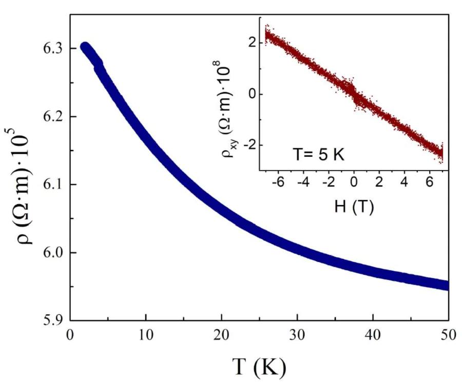
Epitaxial SrIrO\(_3\) and Sr\(_2\)IrO\(_4\) films were grown on oxide single crystals by magnetron sputtering and pulsed-laser deposition under phase-selective temperature and oxygen-pressure conditions[13-17]. The representative transport sample was a 35-nm SrIrO\(_3\) film grown on (110)NdGaO\(_3\). Its resistivity was measured using the four-probe method, and its transverse Hall resistivity was recorded at 5 K in fields up to \(\pm 7\) T (Figure 1). The carrier density and mobility were evaluated within a single-band approximation.
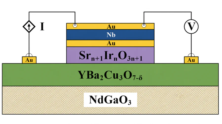
The Josephson devices were fabricated on (110)NdGaO\(_3\) as Nb/SrIrO\(_3\)/YBa\(_2\)Cu\(_3\)O\(_{7-\delta}\) and Nb/Sr\(_2\)IrO\(_4\)/YBa\(_2\)Cu\(_3\)O\(_{7-\delta}\) mesa heterostructures. Typical layer thicknesses were 60-70 nm for YBa\(_2\)Cu\(_3\)O\(_{7-\delta}\), 100-200 nm for Nb, 15 nm for SrIrO\(_3\), and 5 nm for Sr\(_2\)IrO\(_4\). Mesa areas ranged from \(10\times 10\) to \(50\times 50\,\mu\textrm{m}^2\). The upper Nb electrode had a critical temperature of approximately 8.4 K; all junction data reported here were acquired at 4.2 K. The standalone transport film and the junction interlayers originated from related deposition runs. Consequently, the film data identify the conducting, strongly disordered SrIrO\(_3\) regime but are not used as an exact parameterization of each weak link.
Results and discussion
Conducting SrIrO\(_3\) interlayer
The resistivity increases only modestly upon cooling (Figure 1), whereas the Hall response remains approximately linear over the measured magnetic field range. At 5 K, the single-band values were \(n\simeq 1.8\times 10^{21}\,\textrm{cm}^{-3}\), \(\rho\simeq 6.25\times 10^{-3}\,\Omega\cdot\textrm{cm}\), and \(\mu\simeq 0.56\,\textrm{cm}^2/(\textrm{V}\cdot\textrm{s})\). These values place the film in a high-carrier-density, low-mobility regime. This behavior is consistent with the strong sensitivity of SrIrO\(_3\) transport to synthesis, strain, disorder, and quantum corrections reported by independent groups and in our film series[18, 4-8, 13-16]. The weakly nonmetallic slope should therefore not be treated by itself as evidence for an excitation gap.
A \(50\times 50\,\mu\textrm{m}^2\) junction with a 15-nm SrIrO\(_3\) interlayer carried \(I_c\simeq 140\,\mu\textrm{A}\) and had \(I_cR_N\simeq 0.1\,\mu\textrm{V}\). The central part of \(I_c(H)\) is described by the standard Fraunhofer expression with a maximum critical current \(I_0 = 138.5\,\mu\textrm{A}\), a magnetic field period \(\Delta H_0 = 10.9\) Oe, a magnetic field shift \(H_{\rm off} = 1.2\) Oe, and a negligible fitted background (Figure 2).
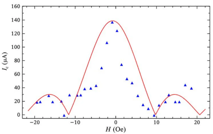
The measured zero-voltage current is predominantly phase coherent. The offset is compatible with residual field or trapped flux, while the unequal side lobes can arise from current-density inhomogeneity, the in-plane lead geometry, and flux focusing[19, 20]. The fit reproduces the central lobe and its first minima, the features most directly determined by the effective junction area. The residual deviations are therefore more naturally associated with a nonuniform spatial distribution of the supercurrent than with a loss of phase coherence. Similar nonideal diffraction patterns are common in finite-size junctions with nonuniform current density[19, 20].
With a current density \(J_c\simeq 5.6\,\textrm{A/cm}^2\) and an assumed magnetic thickness \(d_{\rm eff}\simeq 250\,\textrm{nm}\), the Josephson penetration depth is estimated as
The resulting \(\lambda_J\) exceeds the 50 \(\mu\textrm{m}\) junction width. Self-field effects are therefore unlikely to be the dominant source of the observed asymmetry.
Insulating Sr\(_2\)IrO\(_4\) interlayer
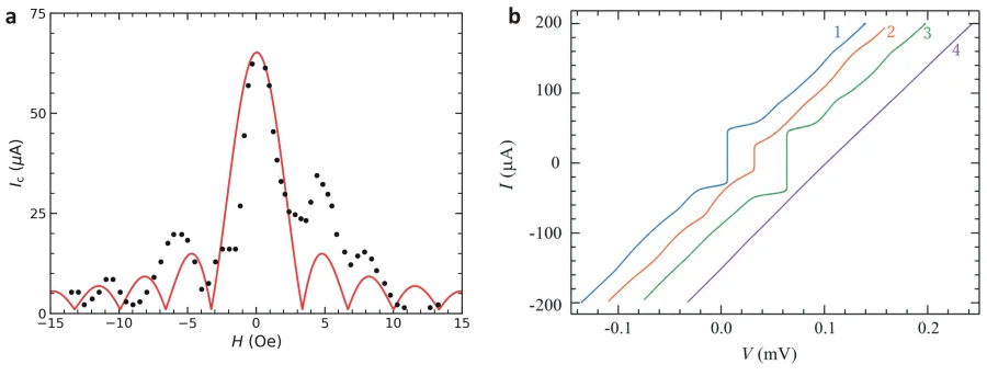
The 5-nm Sr\(_2\)IrO\(_4\) interlayer produced a markedly different normal-state resistance scale while retaining Josephson coupling. For \(40\times 40\,\mu\textrm{m}^2\) and \(20\times 20\,\mu\textrm{m}^2\) devices, \(I_cR_N\) reached 41 and 79 \(\mu\textrm{V}\), respectively. The magnetic diffraction pattern of the larger junction was fitted with a maximum critical current \(I_0 = 64.2\,\mu\textrm{A}\), a field period \(\Delta H_0= 3.32\) Oe, a magnetic field shift \(H_{\rm off} = 0.05\) Oe, and a small background of approximately 1 \(\mu\textrm{A}\) (Figure 3a). The current-voltage curves contain field-dependent resonant steps (Figure 3b). These features are identified as Fiske steps, which result from resonant coupling of the ac Josephson oscillation to electromagnetic modes of the junction[12, 19, 21]. The area-normalized normal resistance \(R_NA\) of the Sr\(_2\)IrO\(_4\) devices was approximately \(9\times10^{-6}\,\Omega\cdot\textrm{cm}^2\), about 200 times larger than that of the SrIrO\(_3\) devices.
Together with the much larger \(I_cR_N\), this contrast is consistent with two distinct weak-link regimes: a dissipative conducting interlayer for SrIrO\(_3\) and a tunnel barrier for Sr\(_2\)IrO\(_4\). Because the two device sets differ in interlayer thickness and fabrication details, the comparison is used to establish the transport regime rather than to extract a unique microscopic interface transparency.
Across the measured devices, \(I_cR_N\) ranged from \(0.1-0.3\,\mu\textrm{V}\) for SrIrO\(_3\) and \(41-79\,\mu\textrm{V}\) for Sr\(_2\)IrO\(_4\), while \(R_NA\) ranged from \((3-8) \times 10^{-8}\) to \((0.8-1)\times 10^{-5}\,\Omega\cdot\textrm{cm}^2\), respectively. Thus, despite differences in geometry and interlayer thickness, both observables consistently distinguish the conducting and insulating weak-link regimes.
The small field offset and unequal side lobes in Figure 3a should not be interpreted by themselves as evidence for an unconventional current–phase relation. As in the SrIrO\(_3\) junction, residual field, flux focusing, and spatial variations of the current density can produce nonideal diffraction patterns[19, 20]. The field-dependent resonant structure in Figure 3b provides an independent dynamical signature of Josephson coupling through its connection with cavity modes of the junction[19, 21].
Conclusion
Josephson transport was observed through both conducting SrIrO\(_3\) and insulating Sr\(_2\)IrO\(_4\) thin-film interlayers in Nb/iridate/YBa\(_2\)Cu\(_3\)O\(_{7-\delta}\) mesa heterostructures. The SrIrO\(_3\) interlayer combines high carrier density with low mobility and yields a low-voltage, strongly damped weak link. By contrast, the Sr\(_2\)IrO\(_4\) interlayer increases both the characteristic voltage and the area-normalized normal resistance by about two orders of magnitude. The magnetic diffraction patterns confirm phase-coherent supercurrent; their asymmetries can be explained by residual or trapped flux.
Acknowledgements
The authors thank V. A. Baydikova, I. E. Moskal and K. E. Nagornykh for experimental assistance and useful discussions. This work is dedicated to the memory of Karen Y. Constantinian, a talented scientist, wise mentor, and remarkable person, whose contributions were essential to the development of this research. His scientific insight, profound knowledge, and dedication to science will always be remembered by his colleagues and students.
This study was carried out under State Assignment No. FFWZ-2025-0009 at the Kotelnikov Institute of Radio Engineering and Electronics of the Russian Academy of Sciences.
Contact information
Corresponding author: N. V. Dubitskiy, orcid.org/0009-0003-1723-8103, e-mail: nikita.dubitskiy@gmail.com
* This paper is based on a talk presented at the II International Scientific Conference “Advanced functional materials for digital and quantum electronics 2026”, September 14–18, 2026, Dolgoprudny, Russia.
Funders
References