


Keywords
Abstract
We recently demonstrated that the dielectric permittivity of a single-layer SrTiO3 thin film decreases with increasing thickness, and that incorporation of intermediate AlFeO3 layers into an SrTiO3 /AlFeO3 heterostructure mitigates this suppression of dielectric properties. We proposed two temperature-dependent mechanisms that could contribute to this effect: thermal strain and the formation of polar nanoregions (PNRs). In this study, we used Raman spectroscopy to assess the possibility of PNR formation in single-layer SrTiO3 films (50 and 250 nm thick) and in a multilayer heterostructure 5×[50 nm SrTiO3 + 50 nm AlFeO3 . Our results show that the spectra of SrTiO3-containing structures exhibit telltale signs of PNR formation: the presence of symmetry-forbidden first-order modes and an asymmetric shape of the TO2 mode.
Introduction
In recent years, heterostructures have attracted a great deal of attention within the field of materials science. This is because they offer a means to combine different functionalities within a single heterostructure, thus enhancing or fine-tuning the properties of individual layers, and sometimes even giving rise to entirely new phenomena. Compelling examples of the benefits of superlattice design are multiferroic and magnetoelectric composites, in which the alternation of magnetic and ferroelectric layers leads to the coupling between electric polarization and magnetization \cite{Paper-1}.
Although single-phase multiferroics do exist, they are relatively rare and are subject to certain fundamental constraints. For example, in the context of perovskite multiferroics the so-called \( d^0-d^n \) problem has been identified. The issue arises from incompatible requirements for the electron configuration of ferroactive (\( d^0 \)) and magnetic (\( d^n \)) ions, which limit the ways of creating multiferroics \cite{Paper-2}. Conversely, artificial heterostructures based on two materials --- one with strong magnetic response and one with strong ferroelectric response, are free from these constraints. Popular choices for this purpose are magnetic materials such as TbDyFe2 (Terfenol-D) [\citeonline{Paper-3}], Ni0.8Zn0.2Fe2O4 [\citeonline{Paper-4}], La0.7Sr0.3MnO3 [\citeonline{Paper-5}], and ferroelectrics such as Pb(Zrx,Ti{1-x})O3 [\citeonline{Paper-3}-\citeonline{Paper-5}], Pb(Mg0.33Nb0.67)O3–PbTiO3 [\citeonline{Paper-6}], BaTiO3 [\citeonline{Paper-7}].
Strontium titanate (SrTiO3, STO) is a quantum paraelectric, which has exceedingly high intrinsic dielectric permittivity at low temperatures \cite{Paper-8}. Although pristine STO crystal does not undergo ferroelectric phase transition at any temperature, there are numerous ways to induce such a transition, including mechanical strain and chemical modifications \cite{Paper-9,Paper-10}. Materials based on STO are frequently used as a part of multiferroic heterostructures and superlattices owing to their robust dielectric response and low dielectric losses across a wide frequency range from DC up to sub-THz band \cite{Paper-10,Paper-11,Paper-12}. In addition, several intriguing phenomena arise at the interfaces between STO and other compounds. For example, two-dimensional electron gas emerges between the layers of LaAlO3/SrTiO3 heterostructure \cite{Paper-13}, and alternation of PbTiO3 and SrTiO3 layers induces improper ferroelectricity in the bicolor superlattice \cite{Paper-14}.
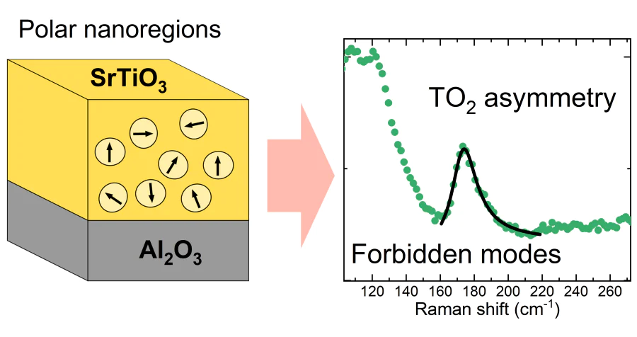
Recently, we reported that incorporation of intermediate layers of AlFeO3 (AFO) between thin layers of STO in STO/AFO superlattice mitigates the suppression of the terahertz (THz) dielectric response of the STO\cite{Paper-15}. The AFO was selected as a material for intermediate layers due to its transparency in THz frequency range, so that the dielectric response of the heterostructure is determined exclusively by STO properties. AFO ceramics are known to exhibit multiferroic properties\cite{Paper-16,Paper-17}. They possess a ferrimagnetic structure with a Neel temperature \( T_N=250 \) K and undergo a ferroelectric phase transition at \( T_P=103 \) K [17]. We proposed two main mechanisms to explain the observed enhancement of the dielectric response, namely, different thermal strain on the STO/AFO and STO/Al2O3 interfaces and formation of polar nanoregions (PNRs) within the STO layers. The temperature-dependent change in the dielectric constant through a strain-related mechanism is caused by an increase in the ferroelectric transition temperature \cite{Paper-18}. The formation of PNRs in STO thin films leads to a substantial increase in the TO1 mode frequency \cite{Paper-19}, which, in turn, leads to a dramatic decrease in the mode’s contribution to the static permittivity. TO1 mode is the ferroelectric soft mode of STO and contributes up to 99% of its static permittivity\cite{Paper-12}, meaning that the static permittivity is affected accordingly. The accumulation of thermal strain is self-evident given that the growth temperature is significantly higher than the ambient temperature and significantly lower than the melting points of STO and AFO. The existence of PNRs, however, needs substantial evidence. One of the hallmarks of the PNRs formation in STO is the emergence of symmetry-forbidden first order vibrational peaks in Raman spectra \cite{Paper-20}.
In this paper, we present the results of a room-temperature Raman spectroscopic investigation of STO/AFO heterostructure and single layer STO and AFO films deposited on (0001) Al2O3 substrates. We demonstrate that the spectra of SrTiO3-containing structures exhibit symmetry-forbidden first-order modes and an asymmetric TO2 mode, both observations suggest the formation of polar nanoregions in SrTiO3.
Experiment
Epitaxial films of AFO and STO were grown on the \( \alpha \)-Al2O3 (0001) substrates by means of pulsed laser deposition. The growth was carried out from AFO and STO stoichiometric targets ablated by pulsed radiation of a KrF excimer laser COMPex Pro (\( \lambda = 248\, \)nm, Coherent Corp., Saxonburg, PA, USA). The growth was performed in the SURFACE Advanced pulsed laser deposition (PLD) setup (SURFACE systems + technology GmbH & Co. KG, Hueckelhoven, Germany). The substrates were attached to a stainless-steel sample holder that was radiatively heated from the back with a platinum filament. The temperature of the sample holder was measured with a type-K thermocouple. The growth was performed at 800^{\circ}C in an oxygen atmosphere at a pressure of 0.02 mbar. The growth rate was close to 0.5 nm/min calibrated by means of Inficon quartz thickness monitor (INFICON Holding AG, Bad Ragaz, Switzerland). The details and results of X-Ray diffraction characterization of the samples are presented elsewhere [\citeonline{Paper-15}]. In all samples, STO layers were found to be textured with cubic perovskite structure (\( Pm\bar{3}m \)) and preferential orientation (111). AFO layers were found to have \( Pna2_1 \) structure without any preferential orientation.
![[{"id":"GplM0_WLzC","type":"paragraph","data":{"text":"<b>a-c</b> - SEM images of the 50-nm-thick STO film (panel <b>a</b>), 250-nm-thick STO film (panel <b>b</b>) and 5\\( \\times \\)[50 nm SrTiO<sub>3</sub> + 50 nm AlFeO<sub>3</sub>] STO/AFO heterostructure on Al<sub>2</sub>O<sub>3</sub> substrates (panel <b>c</b>). All values correspond to the nominal thicknesses of the films. The scale bars (white) in all panels represent 120 nm."}}]](/storage/images/resized/SpAvoHk52rlo3TWs6qEIjWI3vpvh8u0y2k17bTGt_xl.webp)
Post-growth room-temperature thicknesses of all layers were extracted from scanning electron microscopy (SEM) images (Figure 1.). The cross-sections of the samples were prepared on a Helios G4 PFIB UXe dual-beam system (Thermo Fisher Scientific, MA, USA) using a focused Xe+ ion beam (FIB). Prior to FIB milling, a conductive carbon layer was sputtered with a Quorum Q150R ES magnetron (Quorum) followed by deposition of a protective Pt layer inside the Helios column. The films were imaged in an immersion mode at 5 kV and 13 pA. Their thickness was measured at several points of the cross-section taking into account the tilt correction. The single layer STO films with nominal thicknesses of 50 and 250 nm have real thicknesses of 61\( \pm \)2 nm and 261\( \pm \)3 nm. Layers of the 5\( \times \)[50 nm SrTiO3 + 50 nm AlFeO3] heterostructure have thicknesses of 50\( \pm \)4 nm. In this paper, we designate samples using nominal thicknesses and compositions. More thorough characterization of these films can be found in Ref. [\citeonline{Paper-15}].
Room-temperature Raman spectra were measured with a Horiba LabRAM HR Evolution (HORIBA Ltd., Kyoto, Japan) confocal Raman microscope equipped with Soptop LMPPlan 100\( \times \)0.8 infinity-corrected plan achromatic objective. The excitation laser wavelength was 532 nm and the spot size was about \( 1.8\,\mu \)m2 with the excitation power density of \( 130\, \)kW/cm2. Diffraction grating with 600 lines/mm was used for the measurement in 100-1700\,cm\( ^{-1} \) frequency range. Signal accumulation time for each measurement was 120 s. Several spectra were acquired from each sample, and their variation was negligible.
Results and Discussion
![[{"id":"azHwZlQFny","type":"paragraph","data":{"text":"<b>{a}</b> -- Room-temperature Raman spectra of the 5\\( \\times \\)[50 nm SrTiO<sub>3</sub> + 50 nm AlFeO<sub>3</sub>] (STO/AFO) heterostructure and of single films of AFO (50 nm thick), STO (50 and 250 nm thick), and bare Al<sub>2</sub>O<sub>3</sub> substrate. Peak positions are indicated by numbers and, for known STO lines, by their vibrational mode. The spectra are spaced along vertical axis for clarity. <b>{b--d} </b>-- Enlarged views of the STO TO<sub>2</sub> mode. Dots represent experimental data, and black lines show least-square fit with Breit-Wigner-Fano expression (\\ref{Breit})."}}]](/storage/images/resized/ynbqPbTzrUXBVcYcxvGVtJcXMNYtjbso1SFKPdo1_xl.webp)
Figure 2. shows the Raman spectra of the bare Al2O3 substrate, the 50 nm thick SrTiO3 film, the 250 nm thick SrTiO3 film, the 50 nm thick AlFeO3 film, and the 5\( \times \)[50 nm SrTiO3 + 50 nm AlFeO3] heterostructure. The spectrum of the substrate comprises a set of narrow Raman peaks at 380, 418, 450, 578 and 752 cm-1 resting on a smooth background. The peak positions are in full agreement with the literature data for (0001)-cut synthetic sapphire \cite{Paper-21}. Small peak widths (minimal for the diffraction grating used in the setup) indicate that the substrates are of good crystalline quality. The same peaks with slightly reduced intensity are visible in every spectrum displayed in Figure 2., indicating that the laser radiation passes through all layers down to the substrate, and the scattered signal is collected from the films’ volume rather than merely their surface.
In cubic perovskites, such as STO, at room temperature, all first order Raman scattering processes are symmetry-forbidden. The typical spectra of the bulk single crystals primarily consist of two broad second-order scattering bands located at 200-400 cm-1 and 600-800 cm-1 [\citeonline{Paper-22}]. We did not detect any features at these frequencies in the spectra of STO films. Instead, in addition to the signal from the substrate, all STO spectra exhibit two peaks at 175 cm-1 and 810 cm-1. These frequencies coincide with TO2 and LO4 phonon modes of the STO. The spectrum of 250-nm-thick STO film exhibits two overtones (\( \simeq \) 1300 and 1600 cm-1) and an additional peak at 493 cm-1, which does not match any phonon frequency of crystalline STO, but lies close to the LO$^{\,}_2$ mode (475 cm-1 according to [\citeonline{Paper-23}]). Observation of the first order peaks in the spectra of the STO thin films has been documented in the literature \cite{Paper-20,Paper-24,Paper-25}. The widely suggested mechanism of their appearance considers the formation of PNRs. Local distortions of the crystal structure within PNRs remove the symmetry constraints, thereby allowing first-order scattering processes to occur. An additional sign of the formations of PNRs is the characteristic Fano-like shape of the TO2 peak [\citeonline{Paper-24}]. In our measurements, the TO2 mode is slightly asymmetric, which can be most clearly seen in the spectrum of the 250-nm-thick film (figure 1c). We performed least-square fitting of the corresponding peaks with Breit-Wigner-Fano expression:
where \( \omega_0 \) is the central frequency, \( \gamma \) is the line width, \( A \) is the scaling constant and \( q \) is the asymmetry parameter. Fitting the spectra of the 250-nm-thick film and heterostructure shows that the peak is indeed asymmetric with \( q=7\pm 1 \) and 9\( \pm \)3, respectively. In the case of 50-nm-thick film, the peak intensity was too low to allow reliable determination of the value of \( q \).
At room temperature, AFO most commonly possesses one of the two stable crystal structures: orthorhombic (\( Pna2_1 \)) and rhombohedral (\( R\bar{3}c \)) [\citeonline{Paper-26}]. Saha et al. reported the existence of one more orthorhombic phase (\( P2_12_12_1 \)) [\citeonline{Paper-27}]. Previous works on AFO thin films indicate that use of PLD as a growth technique makes \( Pna2_1 \) structure more likely to form, especially if the film is deposited on top of the STO layer \cite{Paper-28,Paper-29}. The Raman spectra of these phases vary greatly \cite{Paper-26}. The most noticeable feature indicative of the rhombohedral phase is the two narrow peaks at 224 cm-1 and 290 cm-1. Our spectrum of 50-nm-thick AFO film has two broad bands located at 700 and 1400 cm-1 along with the peaks from the substrate and weak background curving in the 200-600 cm-1 region. Therefore, we conclude that the film has orthorhombic structure, which is consistent with our XRD results \cite{Paper-15}.
The spectrum of the STO/AFO heterostructure incorporates all the features characteristic to the STO and AFO films with three noticeable differences. Firstly, the peak at 493 cm-1 observed in the spectrum of the 250-nm-thick STO film appears at 540 cm-1, where it coincides with the frequency of TO4 mode. The mechanism of this change requires further analysis. Secondly, in the region 200-500 cm-1, where the spectra of AFO are only slightly curved, several wide overlapping scattering bands appear. Their central frequencies are 230, 280 and 340 cm-1. Thirdly, the 1400 cm-1 peak of AFO is broadened and shifted towards higher frequencies by 30 cm-1. These observations indicate that AFO as a single layer and as a component of heterostructure may have slightly different structure. Judging by the relative intensity of the 200-500 cm-1 band and 700 cm-1 peak, as well as their shapes, the spectrum of AFO in the heterostructure most closely resembles the spectrum reported for \( P2_12_12_1 \) configuration \cite{Paper-26, Paper-27}.
Conclusion
In summary, we performed room-temperature Raman scattering measurements of the 50 nm and 250-nm-thick SrTiO3 films, 50-nm-thick AlFeO3 film and 5\( \times \)[50 nm SrTiO3 + 50 nm AlFeO3] heterostructure grown on \( \alpha \)-Al2O3 (0001) substrate. A single layer of AlFeO3 manifests itself in the spectrum as two scattering bands at 700 and 1400 cm−1 . In contrast, AlFeO3 layers in the heterostructure exhibit several additional peaks located between 200 and 500 cm−1 . The spectra of single SrTiO3 layers feature several first-order modes (TO2 , TO4 and LO4) that are forbidden by the symmetry of the cubic perovskite structure. In the spectra of 250-nm-thick STO film and heterostructure, the TO2 mode exhibits an asymmetric Fano shape. The two observations indicate the formation of polar nanoregions in SrTiO3. This result provides direct spectroscopic evidence of polar nanoregions in SrTiO3/AlFeO3 heterostructures, clarifying the microscopic mechanisms that govern its dielectric behavior. Such observations add to the understanding of quantum paraelectrics and interface-driven phenomena in oxide heterostructures. The insights gained here may prove useful for guiding future efforts to design materials with tailored dielectric or multiferroic properties.